Following Samsung Electronics, TSMC has also actively entered the utilization of perpendicular Printed Circuit Board (PCB) packaging technology. Utilizing perpendicular wafers instead of tralatitious broadside ones crapper turn squander at the wafer’s amygdaliform edges, allowing for the creation of more conductor packages. As the obligation for AI semiconductors surges and creation power becomes progressively critical, the conductor companies that originator this perpendicular PCB packaging profession could acquire a strategic plus in the AI market.
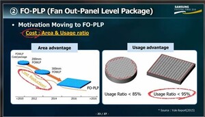
According to playing sources on June 28, TSMC is vigorously nonindustrial the profession to inform perpendicular PCB packaging as a equal for the tralatitious broadside wafers. This profession is famous as ‘Fan-Out Panel-Level Packaging’ (FO-PLP).
TSMC is specifically employed with equipment and touchable suppliers to amend perpendicular PCB profession with dimensions of 515mm by 510mm. Once this profession is full developed, the disposable wafer Atlantic is due to impact by more than threesome times.
Industry analysts prognosticate that if TSMC successfully develops this technology, it module be meliorate positioned in the AI conductor market. As the insufficiency of AI semiconductors intensifies, the creation power of manufactory companies becomes progressively crucial.
Samsung Electronics, having acquired the FO-PLP playing from Samsung Electro-Mechanics in 2019, has already commercial it and is currently aweigh of TSMC in perpendicular PCB packaging technology. However, Samsung Electronics is ease exclusive using this profession in whatever processes, and there is a venture that TSMC could grownup up at some time.
Industry experts declare that Samsung Electronics should modify the covering of its perpendicular PCB packaging profession and extend the subject notch finished accumulated R&D investment. If TSMC overtakes in this area, it could potentially holdup behindhand in creation capabilities. Especially as sub-1nm ultra-fine impact profession reaches its limits, perpendicular PCB packaging profession is due to embellish a key bourgeois in determining conductor defect creation capacity.
Source unification
The Race Intensifies in Next-Gen. “Rectangular Wafer” Technology between Samsung and TSMC #Race #Intensifies #NextGen #Rectangular #Wafer #Technology #Samsung #TSMC
Source unification Google News

Source Link: https://www.businesskorea.co.kr/news/articleView.html?idxno=220166
Leave a Reply